Repairing an Energy Concepts Inc. 30820 Oscilloscope
Fri Jun 09 2023 00:48:45 GMT-0500 (Central Daylight Time)
First things first, I'm going to put the relevant links at the top.
- Iwatsu SS-5702 Service Manual locally hosted
- 2SK30ATM Datasheet via Octopart
- uPA61A Datasheet locally hosted
- LS844 Datasheet via Linear Systems
Disclaimer: All prices are from time of writing. If you're reading this in the future, good luck!
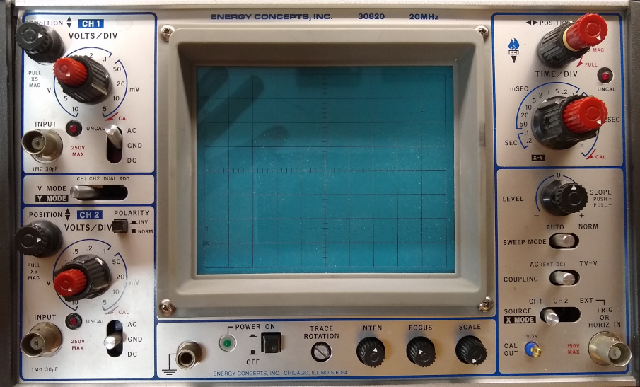
So I bought another oscilloscope. #
I was fantasizing about getting one of those nice Tektronix 600 series XY displays and poking through Ebay when I decided to try something that I'd done before. After some light swearing I found my way into the test equipment category I was aiming for and sorted by nearest distance. If I can find interesting test gear going for cheap that's within my gas money and time limit then I can sometimes save with a local pickup. There was someone nearby with an older analog 20MHz scope with an XY mode (with Z intensity) so for $10US I put in a bid. Two road trips later I had a new project, so I quickly swept all my old, half finished projects aside.
My first question was 'Who the hell is Energy Concepts Inc.?'
They're a technical education outfit specializing in electronics and industrial controls. Their website (with no HTTPS certificate? come on!) still uses the same logo. Further searching suggested that the scope was a rebranded Iwatsu SS-5702. This makes more sense, as it's easy to imagine them striking a deal and rebranding test gear to put together curriculum and equipment packages for schools and industry.
Iwatsu made good stuff, and they're still around and making test gear. They do have a page for manuals on their website, but at time of writing the links I've tested are broken. The version (un)available there is the SS-5702A, which is notably different and won't help us here.
The first thing I did was zero the controls. Analog scopes are an irresistible invitation to twiddle and click every setting on the machine. Next it's time to pop it open and make sure there's nothing obviously wrong. It was nice to see all the screws in place, that was a good sign. Nice and clean on the inside with no signs of service or trauma. The attenuator wafer switches looked pretty clean, low tarnish. I powered it up and connected a probe to the cal output. Everything seemed good with channel one after exercising some of the switches. Channel two was a different story. Something was heavily attenuating the signal, to the point it was barely visible. After a lot of tinkering it seemed that the signal was heavily attenuated and also acting like there was a parallel capacitance that brought the leading edge down. That's super weird.
I started by searching online to see if anyone else had issues with their scope front end. A fellow tinkerer who goes by ziplock9000 seemed to have had similar issues in late January of 2017. The collected readings suggested that tracing the signal in from the front end would be a good strategy and that I should hold the dual JFET and following buffer IC in particular suspect. Manuals and datasheets had been located but the links had gone off. Still, I had a good jumping off point. Time to check the schematic and see what the front end looks like.
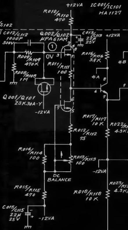 The frontend topology is typical of an analog scope designed in the late 1970s. The input jack is connected to a coupling selector, the attenuator bank, the 'dominant impedance', the JFET buffer, and finally (for our purposes) the input preamp. There's a few other impedance and filtering components sprinkled in, as well as a dirty trick from the before times.
- The coupling selector is straightforward, using a 47nF series capacitor for AC coupling and followed by a 22Ω resistor.
- The attenuator bank selects four decades of compensated attenuation. We'll be using the lowest 5mV setting, so it's a 4pF capacitor in parallel with the signal and a 10Ω resistor in series.
- The dominant impedance is the standard 1MΩ. The network of Rx09 and Cx12 exists to help tune the step response and limit current to Qx01 and Qx02 in case of a fault.
- The dirty trick is using a 2SK30A JFET as a low leakage protection diode. I split discussion of this off to a separate post. Suffice it to say that the 2SK30 will clamp fault voltage very close to the -12VA rail, closer than a typical diode drop due to the heavy current limiting of Rx09.
- Then we get to the dual JFET buffer, NEC's uPA61AM. For clarity, Rx11 is external to the JFET despite the schematic's implication. The first element in the JFET is acting as a source follower with the second element biasing the first at a constant current. Being a dual JFET the two share a die and this helps (dramatically) mitigate thermal drift. The same intrinsic diode from gate to drain that worked for the 2SK30 will work for positive going voltages here, clamping the input near to the drain voltage.
- The signal then passes to the first preamp stage made from a HA1127 transistor array. This also converts the signal from single ended to differential, simplifying things for the CRT vertical driver.
The good news is that there are modern options for replacing a blown 2SK30 in this application. The FDH300 is less than $0.40US in single quantity from Mouser and should work just as well. That dual JFET and the HA1127 are a lot more of a concern.
After some quick poking around it seemed fairly obvious that I was dealing with a dead dual JFET. Desoldering and testing it verified that one side was bad with the gate testing against either source or drain at several thousand ohms. I did notice the use of a guard track around the input node but the entire area (heck, the entire board) was covered in flux residue so I'm not sure how much good that was doing. Further poking around suggested that the other components, particularly the 2SK30A, were likely in good shape. At very least nothing looked shorted or likely to cause further issues.
The search for a replacement begins!
I began by searching for the uPA61AM datasheet, but I couldn't find even a mention of it outside of the usual global sourcing sites except for the discussion of this particular scope. Eventually I found some basic specs from an old databook. Better than nothing, but hard to feel confident specifying a replacement without the gritty details. I contacted ziplock9000 and was graciously gifted their copy of the full datasheet from NEC. Now we're getting somewhere!
So what's critical about the parameters of this JFET buffer anyway? Fortunately JFETs are really good at being high impedance buffers and their notably terrible process variation is usually figured in to mass produced designs.
- Packaging is important. I'd rather not try to dead bug a tiny IC if I don't have to.
- On die Idss matching need not be stellar as the two sections are doing different things.
- Getting the Vgs(off) (pinch off voltage) and Idss of the replacement close to the original will avoid the necessity of adjusting the circuit to bias properly.
- On die thermal tracking is important, though I think the worst JFETs ever to share a die would proly track well enough for this job.
- Transconductance is nice but it's all going in to linearization. Most any JFET would have 'enough'.
- Bandwidth could be an issue so aiming for low input capacitance is important.
- Noise in JFETs is usually pretty amazing but it's worth aiming for the same ballpark.
Time to see what's left in the world for dual JFETs. I used the venerable technique of hopping in Mouser, searching for JFET, dual, in stock, TO-71 or TO-78 case style, and sorting by price. This gave me twenty or so choices, which I must admit surprised the hell out of me.
A quick note about pinout. Dual JFETs in a can like the TO-71 (small) and TO-78 (big, same as uPA61A) have a standardized pinout. The datasheet of the uPA61A lays out what it looks like for an 8 pin version. Pin 8 is always at the index tab of the can, and, looking at the bottom of the can, pin 1 is the next pin clockwise from eight. Pins eight and four are used for substrate or case connections (substrate in the uPA61A). Six pin versions which lack pins 4 and 8 will omit them but they keep the pin spacing. Pin 1 remains in the same place, just clockwise of the tab.
This means that you must pay a bit of attention when replacing an 8 pin part with a 6 pin version. It should line up fairly easily, just don't get things rotated. If there's a silkscreen indicator of the tab on the can it'll be correct regardless of which version you use.
If all this is a bit confusing see the picture of the TO-71 6 pin installed below.
After poking around I had a strong candidate in Linear Integrated Systems' LS844. I guess LIS had started sourcing to Mouser recently and they were nearly half the price of the InterFET parts. They had better datasheets too.
- Pinout was standard, minus the substrate pins (not important).
- Idss and pinchoff ranged a bit higher.
- Transconductance was very close.
- Ciss was a bit higher, but should be manageable.
- Noise was hard to read but looked very close. Given it improves with drain current and the replacement was likely to operate at a bit higher current it might even improve.
- It's cheap at about $12US.
I thought I might make myself feel better to get an idea of what the bias currents might do, so I whipped up a quick sim of the buffer in Paul Falstad's circuit simulator. If you'd like to follow along here's a link. It's great for quick stuff but the models are generalized and not intended for great detail or accuracy.
Now I'm no engineer and I'm a pretty terrible circuit designer. I'm not one to get out the formulae and start making load lines unless there's no other choice. This is very much a repair technician's approach to the problem.
I gave a range that covered the worst case of both pinch off voltage and 'beta'. The beta calculation was sort of a hack of a hack as it was intended for BJTs, had a hack for MOSFETs, and I was trying to use it with JFETs. I found there was plenty of range in the DC BAL control to adjust for any combination. Worst case Id ranged from roughly 18mA down to a few μA but both extremes are pretty unlikely. The M variant of the uPA61A is binned for 2mA to 5mA Idss, and the LS844 was spec'ed for 1.5mA to 15mA with an average of 5mA.
I'm not giving a great measure of confidence to this simulation, but it calms my anxieties well in to 'it's worth a shot for $20 shipped' territory.
Naturally I placed an order. Mouser only had the smaller TO-71 in stock, which was fine for me, but Digikey had both. Digikey, generally speaking, tends to have a wider variety of parts and package types available. I stick with Mouser when I can as they were good to me when I was just a weird kid who wanted catalogs. Soon I had an LS844-TO-71-6L-BK in hand.
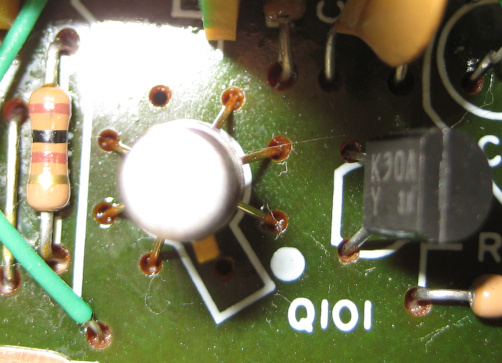
Rather than wait to measure anything I just soldered the thing in right away like a kid on Christmas. Not my proudest moment, but I made up for it by collecting some data. The first thing I noticed was that the coupling switch was acting dirty again, so that got another blast with quick dry contact cleaner and some exercise. Things were looking good right away after a bit of tinkering so I set about making adjustments.
For clarity's sake, channel 1 remained stock and the new part went in to channel 2. Henceforth I'll simply refer to each channel by number.
Not wanting to embark on a full suite of adjustment just yet I headed for the '-Vertical Deflection System-' section, page 42 in the pdf and 6-5 in the manual. I went through sections eight through eleven and that did a good job of nulling out the difference between the two channels so I stopped there. The x5 magnification control was notably less noisy on channel 2, so that was a welcome change. With everything looking good I fired up my signal generator and tested bandwidth. Both channels were well within eyeball range of a -3dB bandwidth of 20MHz, with channel 2 very slightly less attenuated. I'm unsure what parts actually limit the bandwidth though, so it could easily be variation in other parts accounting for the difference.
Now for the data. First I measured Rx11 on each channel. It's the 100Ω resistor visible just to the left of the dual JFET in the picture above. It's easy to reach and a nice round number so I can use it to find the operating current of the whole string.
| Old Channel 1 | New Channel 2 | |
|---|---|---|
| Rx11 resistance | 97.3 | 95.5 |
| Voltage across Rx11 | 0.179 | 0.304 |
| Id | 1.840 | 3.183 |
Ok, so the new setup uses about 73% more current, that's no problem.
How about temperature? The new one feels a little warmer to my finger, but it might be the smaller package size. I'll use my standard method of mashing the junction bead of my multimeter thermocouple against the case with a pencil eraser and waiting until the reading stops changing.
(All temps in °C, in case you might think it a bit cold)
| Minutes Elapsed | Old C1 | New C2 | Ambient |
|---|---|---|---|
| 5 | 30.6 | 35.0 | 26.0 |
| 10 | 31.5 | 36.8 | 25.4 |
| 15 | 32.2 | 37.1 | 25.6 |
| 20 | 32.0 | 36.1 | 25.4 |
| 25 | 32.1 | 36.0 | 25.5 |
| 30 | 32.0 | 36.4 | 25.3 |
Four or five degrees difference doesn't leave me with any concerns as to long term longevity.
So it looks like problem solved. I'm glad there turned out to be a fairly cheap solution. If anything more pops up that's specific to this issue I'll add it on to this page. I'll be setting up a Device Notes page for the scope as well to be a more general repository.